
'/%3e%3cpath%20id='Oval_2'%20fill-rule='evenodd'%20clip-rule='evenodd'%20d='M21.0673%2015.2153C22.9691%2015.2153%2024.5108%2013.7054%2024.5108%2011.8429C24.5108%209.98034%2022.9691%208.47046%2021.0673%208.47046C19.1656%208.47046%2017.6239%209.98034%2017.6239%2011.8429C17.6239%2013.7054%2019.1656%2015.2153%2021.0673%2015.2153Z'%20fill='var(--fill-0,%20%238E62EA)'/%3e%3cpath%20id='Oval_3'%20fill-rule='evenodd'%20clip-rule='evenodd'%20d='M21.0673%2023.9997C22.9691%2023.9997%2024.5108%2022.4897%2024.5108%2020.6271C24.5108%2018.7646%2022.9691%2017.2546%2021.0673%2017.2546C19.1656%2017.2546%2017.6239%2018.7646%2017.6239%2020.6271C17.6239%2022.4897%2019.1656%2023.9997%2021.0673%2023.9997Z'%20fill='var(--fill-0,%20%238E62EA)'/%3e%3cpath%20id='Oval_4'%20fill-rule='evenodd'%20clip-rule='evenodd'%20d='M12.0917%2015.2153C13.9935%2015.2153%2015.5351%2013.7054%2015.5351%2011.8429C15.5351%209.98034%2013.9935%208.47046%2012.0917%208.47046C10.19%208.47046%208.64839%209.98034%208.64839%2011.8429C8.64839%2013.7054%2010.19%2015.2153%2012.0917%2015.2153Z'%20fill='var(--fill-0,%20%235D1EE1)'/%3e%3cpath%20id='Oval_5'%20fill-rule='evenodd'%20clip-rule='evenodd'%20d='M12.0917%2023.9997C13.9935%2023.9997%2015.5351%2022.4897%2015.5351%2020.6271C15.5351%2018.7646%2013.9935%2017.2546%2012.0917%2017.2546C10.19%2017.2546%208.64839%2018.7646%208.64839%2020.6271C8.64839%2022.4897%2010.19%2023.9997%2012.0917%2023.9997Z'%20fill='var(--fill-0,%20%235D1EE1)'/%3e%3cpath%20id='Oval_6'%20fill-rule='evenodd'%20clip-rule='evenodd'%20d='M3.44346%2023.9996C5.34523%2023.9996%206.88691%2022.4897%206.88691%2020.6271C6.88691%2018.7645%205.34523%2017.2546%203.44346%2017.2546C1.54169%2017.2546%201.53543e-06%2018.7645%201.53543e-06%2020.6271C1.53543e-06%2022.4897%201.54169%2023.9996%203.44346%2023.9996Z'%20fill='var(--fill-0,%20%234A18B4)'/%3e%3c/g%3e%3c/svg%3e)

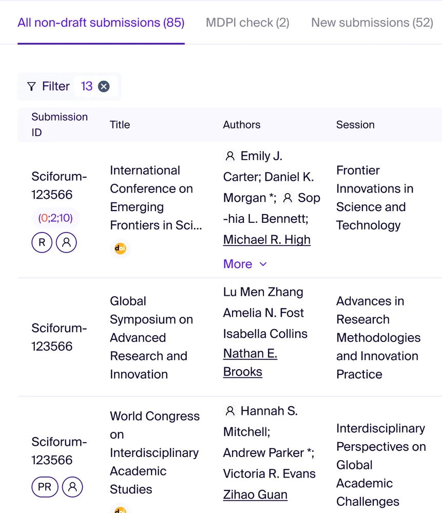

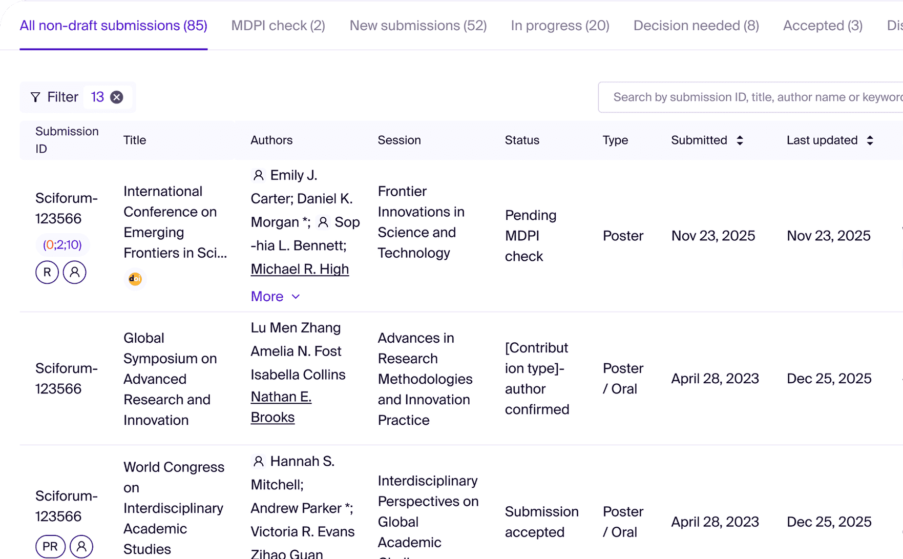
Organize submissions by custom 'Sessions' and assign papers silently to avoid email fatigue. Monitor the decision process directly from a centralized dashboard.
ACADEMIC CONFERENCE MANAGEMENT SOFTWARE
Empowering Science through
Seamless Event Management
From abstract submission to peer review and registration. Modular tools trusted by 1,000+ events worldwide. No hidden fees, and full control over your data.
Manage your
scientific program
From abstract collection To final decision

'%20stroke='var(--stroke-0,%20%23EFE9FC)'%20stroke-width='3.28702'/%3e%3cdefs%3e%3clinearGradient%20id='paint0_linear_0_100'%20x1='16.6717'%20y1='2.1476'%20x2='17.8931'%20y2='28.6822'%20gradientUnits='userSpaceOnUse'%3e%3cstop%20stop-color='%23EFEEFF'%20stop-opacity='0.63'/%3e%3cstop%20offset='1'%20stop-color='%238E62EA'/%3e%3c/linearGradient%3e%3c/defs%3e%3c/svg%3e)

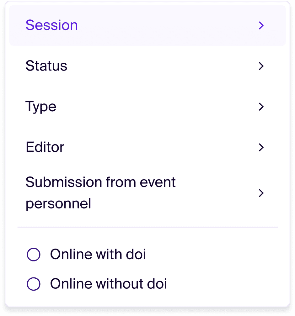
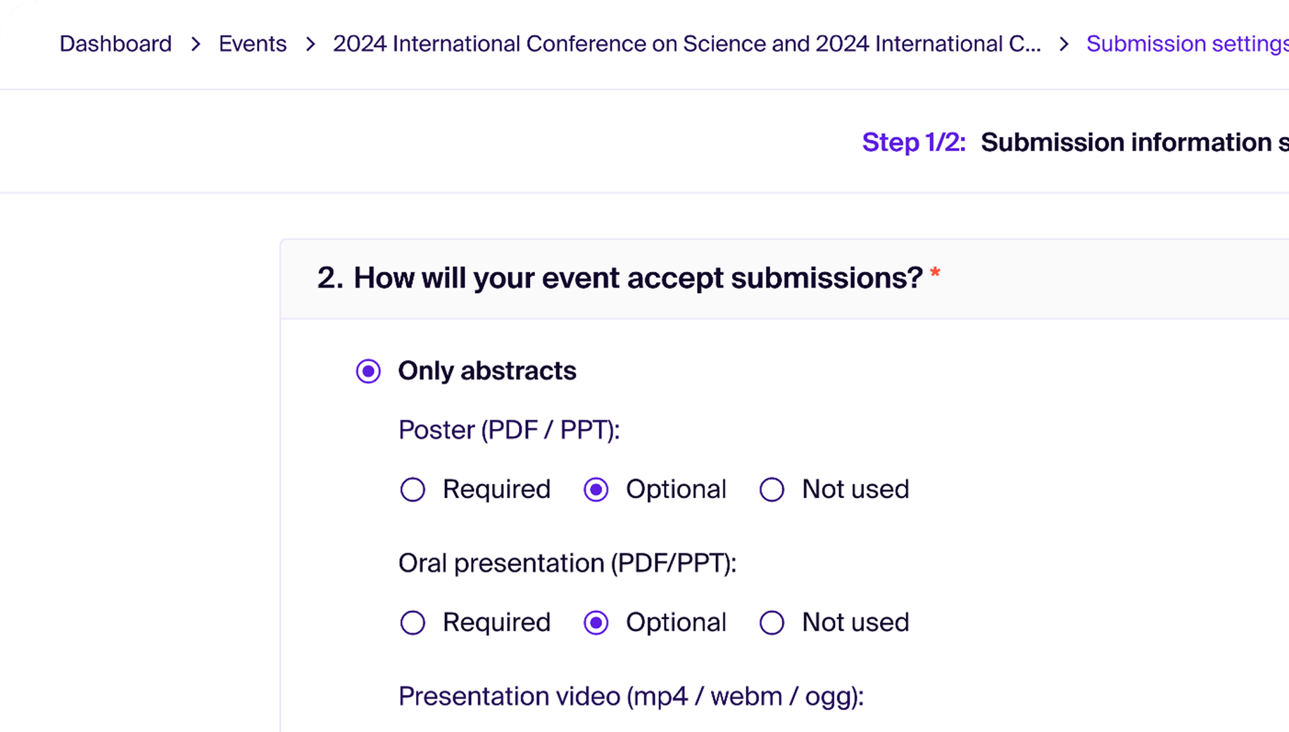
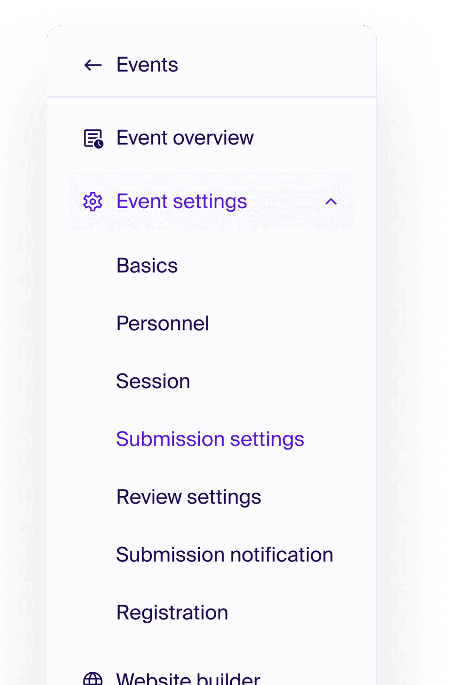
Whether you need simple abstract collection or a rigorous two-stage process (Involving abstracts and full papers), the system adapts to your needs.
Simplify your event's revenue flow
with flexible ticketing and
automated invoicing
Simplify your event's revenue flow
with flexible ticketing and
automated invoicing
Configure a registration structure that fits your specific needs
Easily set up adjustable ticket tiers and offer optional add-ons to enhance the attendee experience. Drive attendance with flexible discount codes.


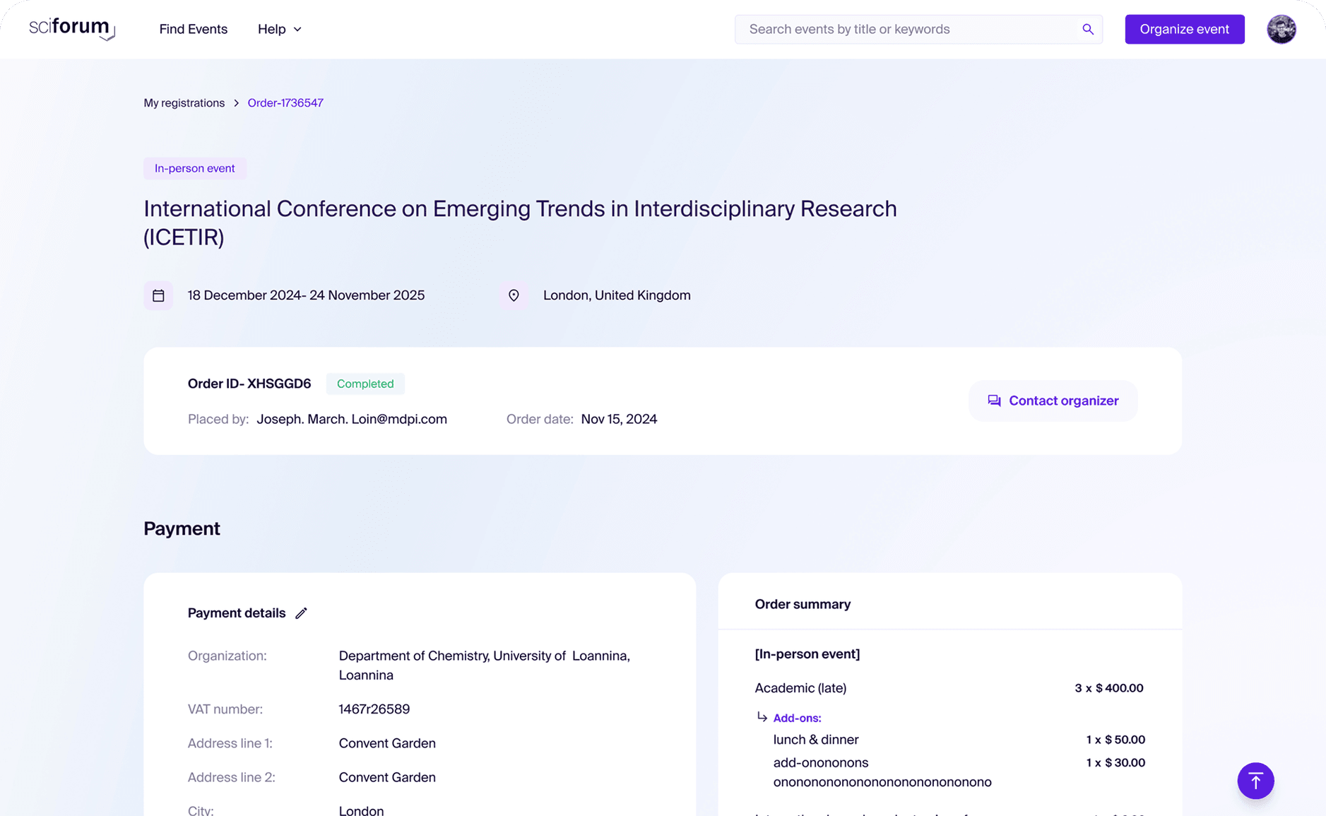
Automate your financial workflow with auto-generated invoices and scheduled payment reminders
Track statuses and accept secure payments easily—while keeping 100% of your revenue via our zero-commission model.

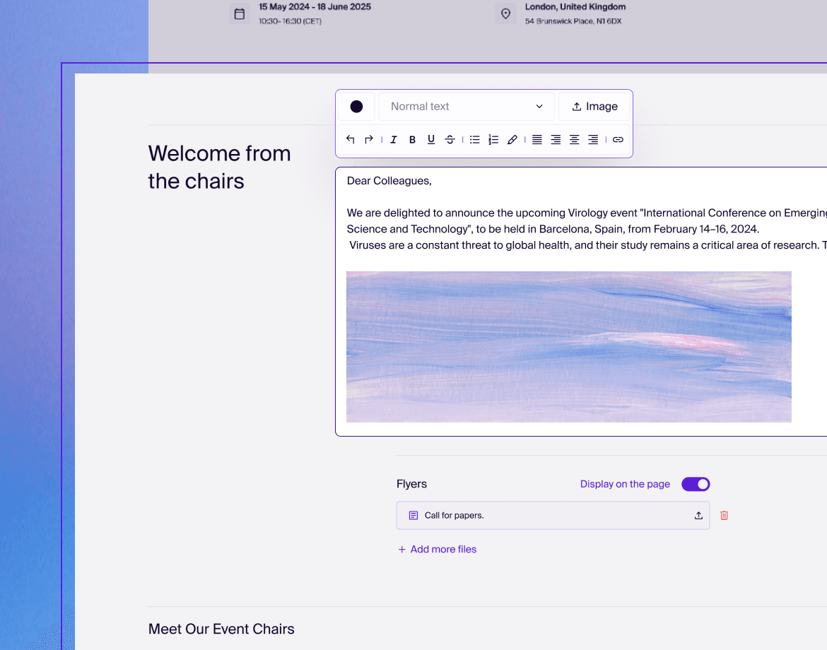
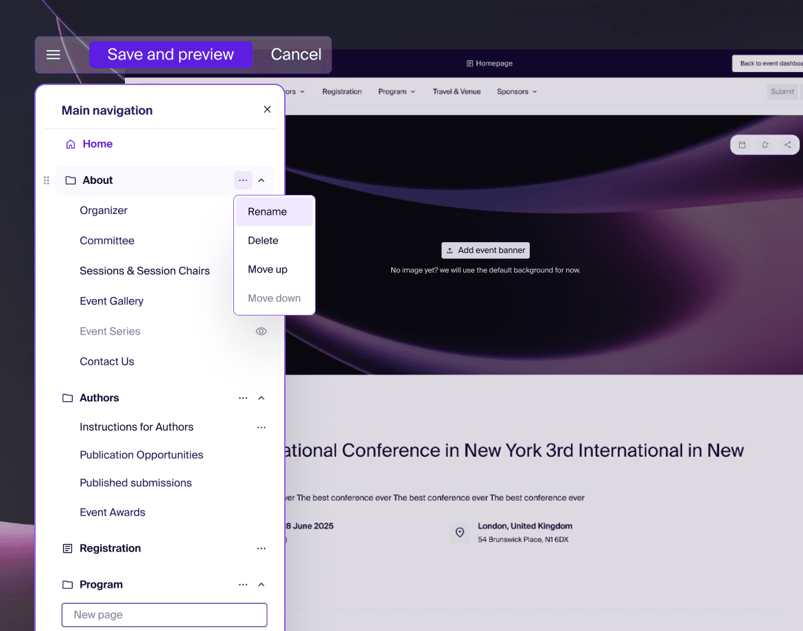
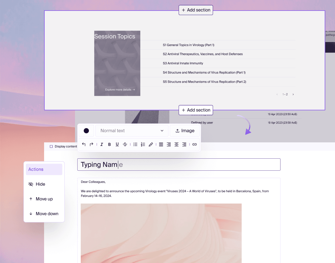
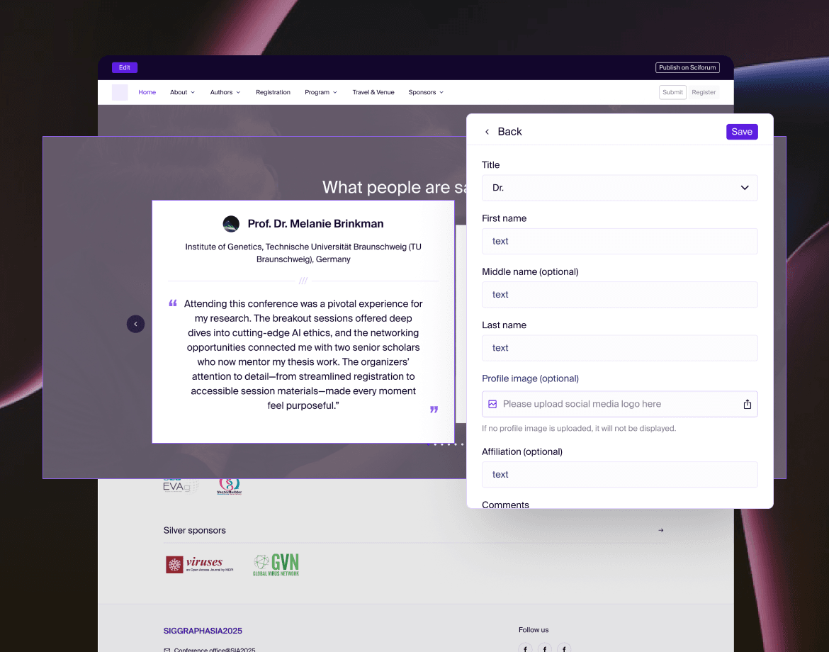
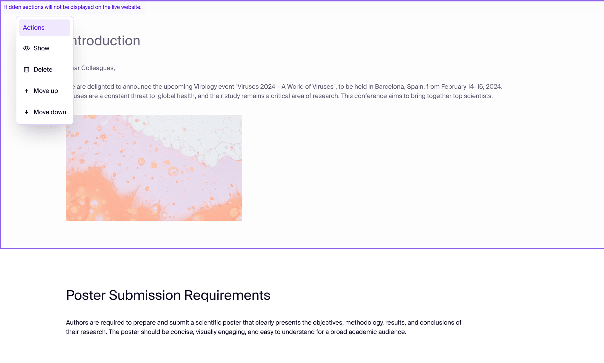
Create a professional, customizable, and permanent event website with ease
Design an event website using dedicated academic templates and our intuitive "what you see what you will get" editor. Customize menus and pages effortlessly to fit your program—with no technical skills required.
Importantly, your website URL remains permanently accessible, preserving your scientific legacy long after the event ends .
Elevate your event with essential
tools for a complete academic experience


Trusted by events worldwide
From focused workshops to major international symposiums, Sciforum supports seamless academic exchange for in-person and virtual events.
1000+
EVENT HOSTED
4,890
SUBMISSIONS
38k+
PARTICIPANTS
53k+
USERS


Ready to host your next academic event?
Get started in minutes with our all-in-one platform built for academia. Join a global community of organizers utilizing efficient management and transparent pricing.
ACADEMIC EVENT MANAGEMENT SOFTWARE
Empowering Science through
Seamless Event Management
From abstract submission to peer review and registration. Modular tools trusted
by 1,000+ events worldwide. No hidden fees, and full control over your data.
Manage your scientific program
From abstract collection To final decision

Streamline review assignments  without
flooding inboxes
without flooding inboxes
Organize submissions by custom 'Sessions' and assign papers
silently to avoid email fatigue. Monitor the decision process
directly from a centralized dashboard.
silently to avoid email fatigue. Monitor the decision process
directly from a centralized dashboard.

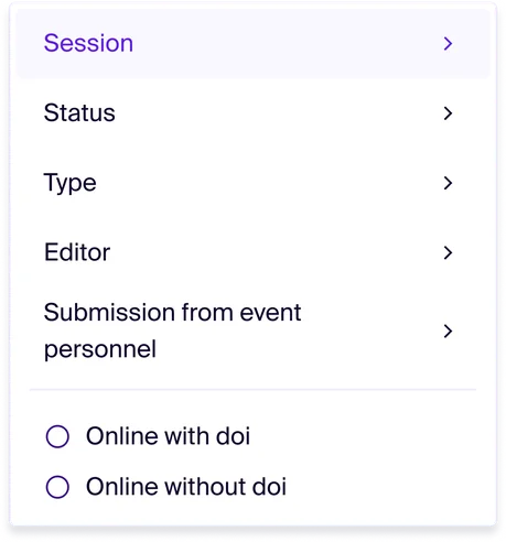
Tailor the submission workflow to your academic
requirements
requirements
'%20stroke='%23EFE9FC'%20stroke-width='3.28702'/%3e%3cdefs%3e%3clinearGradient%20id='paint0_linear_71349_337'%20x1='16.6747'%20y1='3.04015'%20x2='18.0083'%20y2='29.5899'%20gradientUnits='userSpaceOnUse'%3e%3cstop%20stop-color='%23EFEEFF'%20stop-opacity='0.63'/%3e%3cstop%20offset='1'%20stop-color='%238E62EA'/%3e%3c/linearGradient%3e%3c/defs%3e%3c/svg%3e)
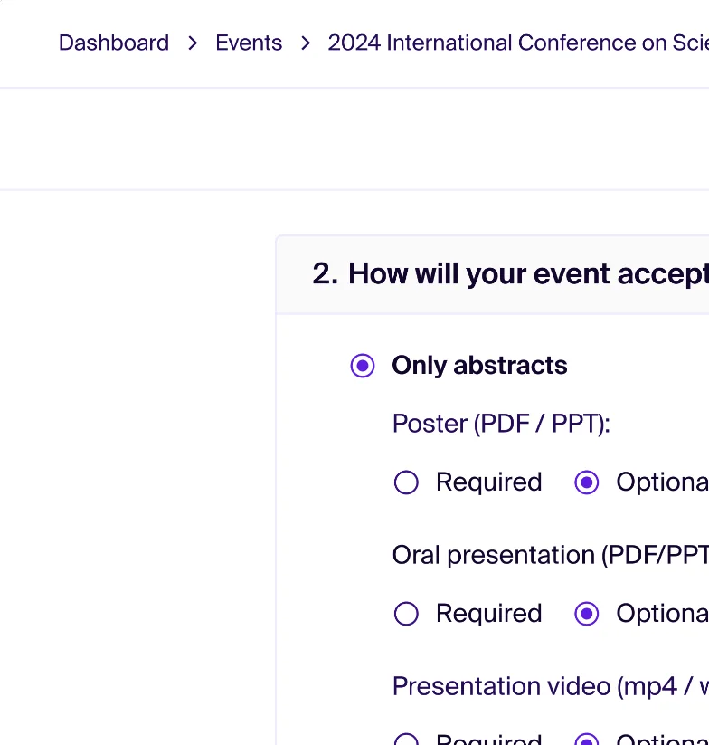
Whether you need simple abstract collection or a rigorous two-
stage process (Involving abstracts and full papers), the system
adapts to your needs.
stage process (Involving abstracts and full papers), the system
adapts to your needs.
Simplify your event’s revenue flow
with flexible ticketing and
automated invoicing
Configure a registration structure that fits your specific needs
Easily set up adjustable ticket tiers and offer optional add-
ons to enhance the attendee experience. Drive attendance
with flexible discount codes.
Automate your financial workflow with auto-generated invoices and scheduled payment reminders
Track statuses and accept secure payments easily—while
keeping 100% of your revenue via our zero-commission
model.
Create a professional,
customizable, and
permanent event website
with ease
Design an event website using dedicated academic templates and
our intuitive "what you see what you will get" editor. Customize
menus and pages effortlessly to fit your program—with no technical
skills required. Importantly, your website URL remains permanently accessible,
preserving your scientific legacy long after the event ends .
Elevate your event with
essential tools for a complete
academic experience
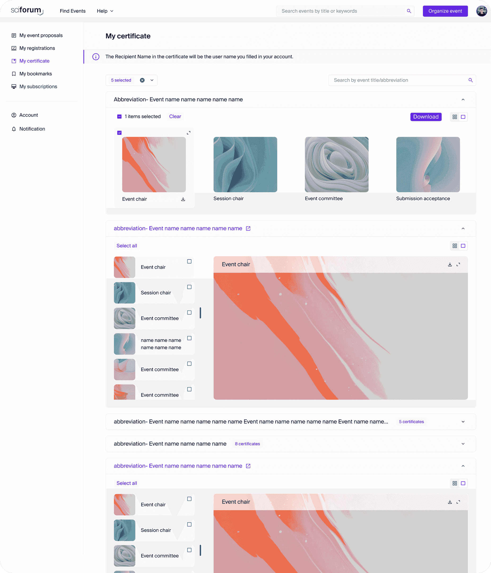
Automated certificates
Automatically generate and distribute certificates of attendance or presentation. Customize templates with your branding and let attendees download them directly.
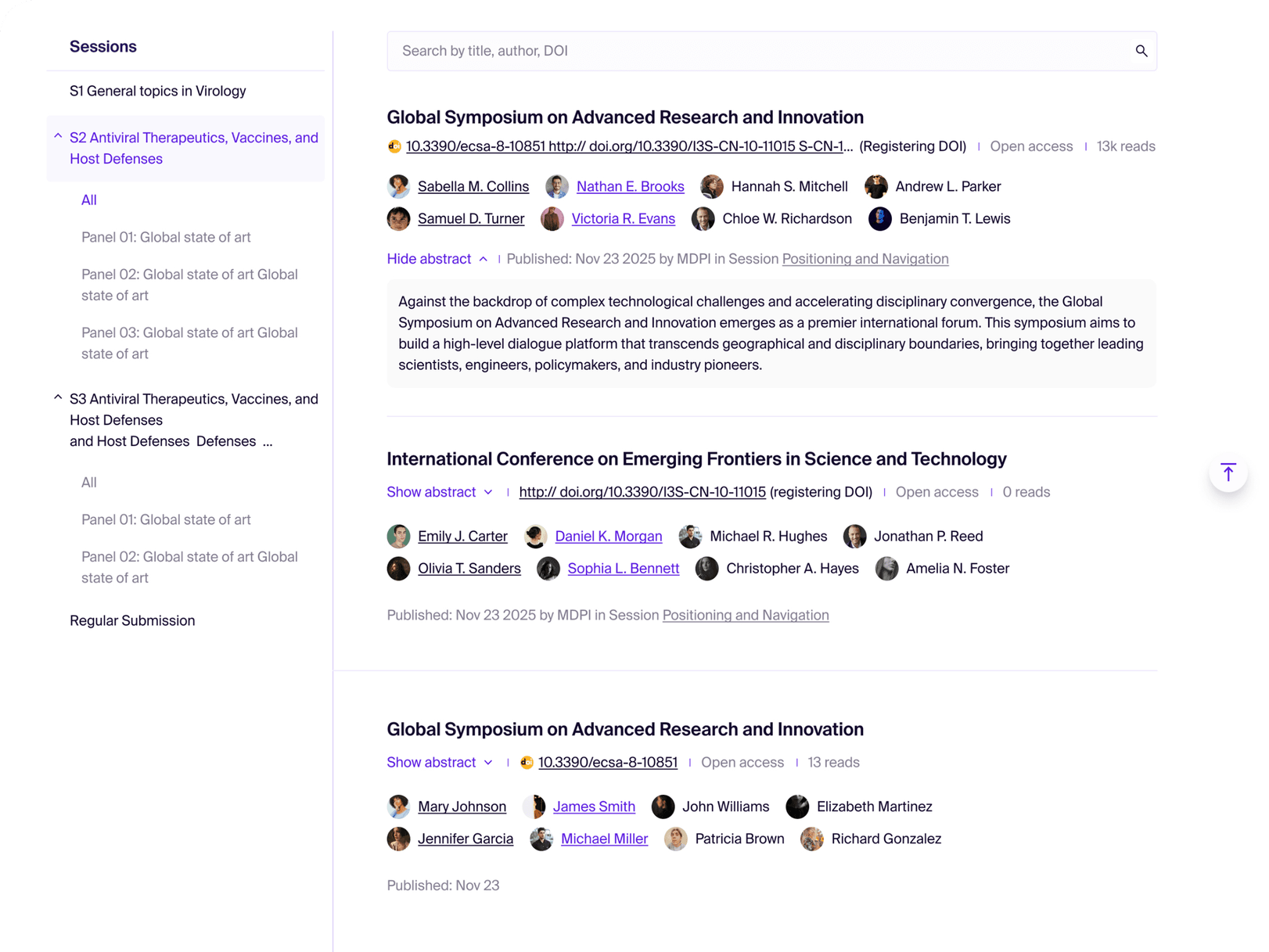
Published submission gallery
Showcase accepted work in a searchable, permanently hosted online gallery. Users can filter by session, search by DOI or author, and access full abstract details instantly.
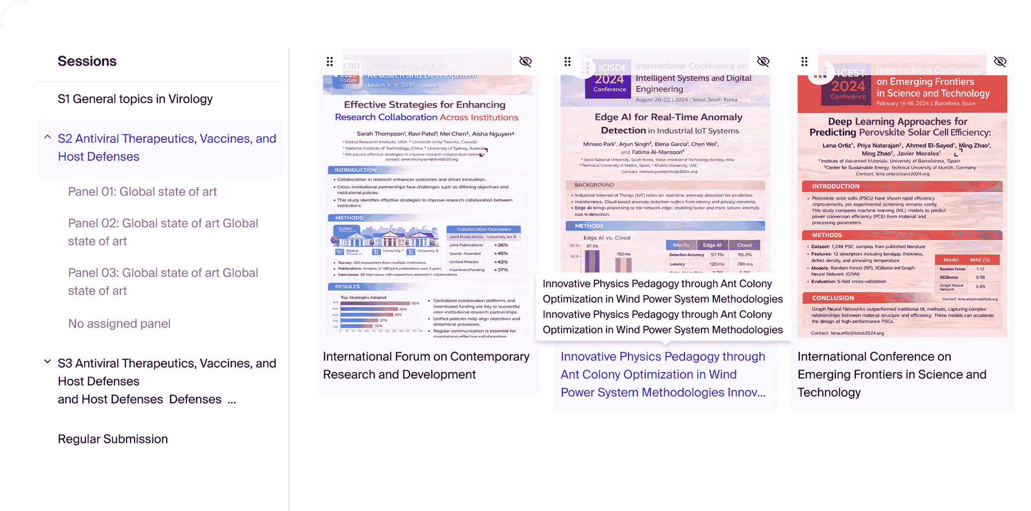
Poster gallery
Sync posters automatically in real-time to a high-quality digital gallery. Let attendees browse research with one click, extending visibility beyond the physical event.

Trusted by events
worldwide
Explore all events
From focused workshops to major international symposiums, Sciforum supports seamless academic exchange for in-person and virtual events.
1000+
EVENT HOSTED
4,890
SUBMISSIONS
38k+
PARTICIPANTS
53k+
USERS
